By Dominic Siriani
A holy grail of photonics and electronics is the integration of silicon CMOS technology with electro-optical devices. In general, this is challenging because mature electro-optic components are made in compound semiconductors, such as GaAs and InP. Development of hybrid integration, where compound semiconductor photonics are combined with silicon electronics using material bonding techniques, is being pursued currently and is a promising approach. Another more direct method, however, is to try to make photonic devices from silicon directly. This is an appealing idea, since silicon is relatively cheap and the microelectronics industry has built up a large technology infrastructure around it.
However, the development of silicon photonic devices poses a number of challenges due to the material properties of silicon. For example, silicon is an indirect bandgap semiconductor, which essentially translates to it being a very inefficient photon emitter. Moreover, the silicon crystal is centrosymmetric (i.e., it has inversion symmetry, so points at (x, y, z) are indistinguishable from those at (-x, -y, -z)), which means it lacks the χ(2) nonlinearity that is responsible for the linear change in refractive index with an applied electric field. What do these two properties mean in practical terms? It takes a lot of ingenuity and hard work to realize two of the most essential electro-optical devices: the laser and the modulator.
Within the past several years, a few breakthroughs have helped develop these devices in silicon. A silicon laser has been created by using the fact that Raman amplification can occur in silicon. Raman amplification occurs as a result of stimulated Raman scattering. Raman scattering is a nonlinear effect that involves a pump photon generating a (typically) lower frequency photon and a phonon. The stimulated version of this effect is similar to that of familiar stimulated emission in lasers: the more signal photons in the material the more rapidly pump photons are converted into signal photons. Thus, amplification occurs, and with sufficient feedback one can make a laser. Although the performance is not at the level of conventional GaAs- or InP-based lasers, it is an encouraging and interesting first step.
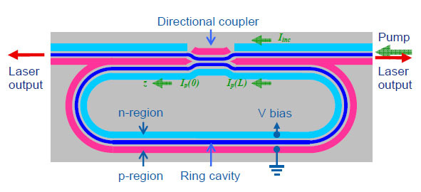 A ring silicon laser based on stimulated Raman scattering nonlinear effects (H. Rong, Y. Kuo, S. Xu, A. Liu, R. Jones, M. Paniccia, O. Cohen, and O. Raday, “Monolithic integrated Raman silicon laser,” Opt. Express 14, 6705-6712 (2006).)
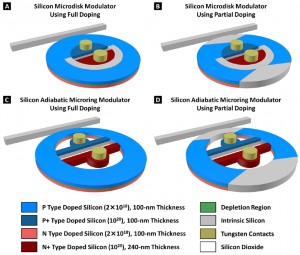 Silicon microring modulators based on the depletion effect (carrier-induced refractive index change) (A. Biberman, E. Timurdogan, W. Zortman, D. Trotter, and M. Watts, “Adiabatic microring modulators,” Opt. Express 20, 29223-29236 (2012).)
The challenge of making a silicon modulator has also been approached in creative ways. In many cases, since the linear electro-optic effect is not present in silicon, other refractive index altering methods are used. The most common approach is to utilize the property that adjusting the carrier concentration changes the refractive index. In this case, one can create a p-n junction and then modulate the reverse bias to change the depletion width, thereby changing the effective index of a mode traveling down a waveguide. This phenomenon has been combined with novel device structures, such as microrings, to make very compact, fast, and efficient silicon modulators. In addition, a more recent development has been to induce the χ(2) nonlinearity in silicon by introducing strain. In this case, strain changes the crystal structure such that the centrosymmetry is broken. Thus, a linear electro-optic effect is introduced, and refractive index changes can be induced by applying an electric field.
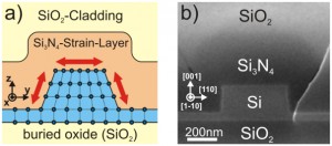 Schematic and SEM images of a strained Si modulator.
(B. Chmielak, M. Waldow, C. Matheisen, C. Ripperda, J. Bolten, T. Wahlbrink, M. Nagel, F. Merget, and H. Kurz, “Pockels effect based fully integrated, strained silicon electro-optic modulator,” Opt. Express 19, 17212-17219 (2011).)
These recent advances give some hope for developing photonic devices directly in silicon. Time will tell what the ultimate solution to bringing electronics and photonics together will be, but it is certain that the challenge has brought about some very ingenious and creative approaches.
Disclaimer: Opinions, interpretations, conclusions, and recommendations are those of the author and are not necessarily endorsed by the United States Government and MIT Lincoln Laboratory.
Posted: 11 March 2013 by
Dominic Siriani
| with 0 comments