By Dominic Siriani
First off, congratulations to the award recipients honored at the Plenary and Awards Session I at Tuesday’s CLEO meeting. The session was highlighted by presentations by Prof. Paul Corkum, who spoke about the development and science of attosecond photonics, and by Prof. Stephen Harris, who gave an excellent history of parametric down conversion. Both talks gave some great insight into the basic science of quantum mechanics and photonics.
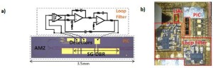 Schematic diagram and image of an integrated negative feedback loop controlled SG-DBR laser capable of producing a linewidth of 100s of kHz, produced by researchers at University of California at Santa Barbara (Sivananthan et al., “Integrated linewidth reduction of a tunable SG-DBR laser,” presented at CLEO, 2013.)
Following the plenaries, I primarily saw talks that revolved around the topic of integrated photonics. In the session “Photonic Integration and Interconnects” (CTu1L), there were a number of excellent presentations on developments in compact components for optical data routing and communication. One talk highlighting the work at IBM described both ring resonator and Mach-Zehnder switches integrated in a CMOS process for on-chip packet routing. Another talk from the University of California at Santa Barbara described the development of a narrow linewidth sampled-grating distributed Bragg reflector (SG-DBR) laser utilizing integrated active feedback control. By implementing a negative feedback control loop with an on-chip Mach-Zehnder frequency discriminator, the group has been able to realize a very fast loop bandwidth and thereby reduce the laser linewidth from 10s of MHz to 100s of kHz while also being able to achieve fast (electronically controlled) wavelength tuning. Also in the session was an invited presentation from the Photonics Electronics Technology Research Association, the National Institutes of Advanced Industrial Science, and the University of Tokyo, all in Japan. This presentation described the hybrid integration of compound semiconductor diode lasers onto a silicon platform with mode converters, modulators, and photodiodes for high bandwidth density interconnects.
In a later session, I also saw a tutorial by Dr. Yurii Vlasov of IBM on integrated silicon nanophotonics for chip-to-chip interconnects. Dr. Vlasov discussed how integrated silicon photonics has been around for decades, but it is just recently that it seems there might be an actual need for the technology in order to keep up with the ever-increasing data traffic. He pointed out how techniques for scaling electronic chip-to-chip links begin to consume too much space and power as bandwidth is increased, and this drives a need for photonic interconnects. However, photonic interconnect cost needs to be driven down in order to make this a practical or even feasible solution, and one way to do so is to incorporate silicon photonics into the existing CMOS foundation. He then described the efforts at IBM to do this, including the incorporation of photodiodes, modulators, and wavelength division multiplexers into their CMOS foundry. He concluded by referencing an observation that many technologies undergo a period of hype, followed by a backlash of disillusionment, and then finally, if the technology is relevant, sustained interest and technological growth. He noted that integrated silicon photonics seems to be at the peak of its hype and a sharp drop in the appeal is likely to come. However, due to long-term scaling needs that are apparent from new high-bandwidth data communication standards, it seems likely that integrated silicon photonics will be the type of technology to experience the revival of interest and sustained growth that is experienced by most stable commercial technologies.
Disclaimer: Opinions, interpretations, conclusions, and recommendations are those of the author and are not necessarily endorsed by the United States Government and MIT Lincoln Laboratory.
Posted: 12 June 2013 by
Dominic Siriani
| with 0 comments