By Dominic Siriani
Looking over the advance version of the CLEO 2013 conference program, I couldn’t help but notice an interesting trend in the “Semiconductor Lasers” invited speakers list: all of the topics cover what I’ve considered to be “unconventional” semiconductor lasers. Photonics crystals, diamond emitters, plasmonics, polariton lasers, and quantum cascade lasers typically don’t come to my mind when I think of semiconductor lasers. I sat back and contemplated this. Maybe these should pop into my head. After all, a consequence of scientific research is the continuous evolution of ideas and technologies. This might just be part of the new look of semiconductor lasers.
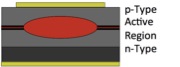 Conventional edge-emitter viewed from facet.
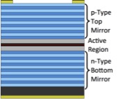 Conventional VCSEL viewed from side.
I probably should explain my perspective. Despite being exposed to and having even worked a bit with these “unconventional” lasers, my training has bred the perception that semiconductor laser is synonymous with diode laser; that is, semiconductor laser = active region (quantum wells) + p-n junction. The properties of the emitted light are determined primarily by the semiconductor material (band structure, which determines energy of the interband transition producing light, and such) and to some degree by the physical structure (well width, waveguide geometry, etc.). The wells could be inside a waveguide (an edge-emitter) or between distributed Bragg reflector stacks (a vertical-cavity surface-emitting laser). These are really the mature semiconductor diode laser paradigms that are found all over the place, in industry and science, and they have been (and continue to be) the topic of significant research for decades.However, simultaneously, there has been a movement to meld the attractive and unique aspects of semiconductors with novel phenomena. These include the aforementioned topics to be discussed by the CLEO invited speakers. Most of these are relatively new ideas that push the envelope of what semiconductor emitters can do. (Granted, it can be argued that quantum cascade lasers are fairly well established at this point, but they still break from the typical diode laser prototype since they rely on intersubband emission in a quantum well superstructure). And what all of these have in common is that they are approaches to move semiconductor photonics to regimes that were previously inaccessible (i.e. different wavelengths, smaller size, stronger light-matter interaction, etc.).
The tutorial subject illustrates what I consider to be a quintessential example of evolving semiconductor laser technology: photonic crystals. Susumu Noda, a professor at Kyoto University in Japan and expert on photonic crystal lasers, will conduct the tutorial. In a sense, photonic crystals are the ultimate manipulators of light, due to the flexibility of their design and the various photonic properties they can influence. Photonic crystals can alter light emission, propagation, and matter interaction (including absorption/gain, nonlinear effects, etc.). Combining the photonic manipulations enabled by photonic crystals with the light-matter interactions produced by semiconductors allows researchers to think about novel effects, such as thresholdless lasing and enhanced gain and absorption. It has helped create some serious thought about ultra-compact optical buffers, optical memory, and quantum photonic computing. Photonic crystals have definitely infused some new thought into the realm of semiconductor lasers.
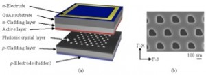 Photonic crystal incorporated into semiconductor laser structure (Yoshitaka Kurosaka, Kazuyoshi Hirose, Akiyoshi Watanabe, Takahiro Sugiyama, Yong Liang, and Susumu Noda, “Effects of non-lasing band in two-dimensional photonic-crystal lasers clarified using omnidirectional band structure,” Opt. Express 20, 21773-21783 (2012)).
What defines a “semiconductor laser” is certainly evolving. As more is learned about what goes on at the nano-scale and in the quantum world, semiconductor lasers encompass more variety of physical structures and phenomena. And this potentially has been true for a while, but no longer can one simply consider the p-n diode with an active region when thinking of semiconductor lasers. Semiconductor lasers have been taking on some new looks, and with that, they’ve also added some remarkable new abilities. Stay tuned to CLEO 2013 for more.
Disclaimer: Opinions, interpretations, conclusions, and recommendations are those of the author and are not necessarily endorsed by the United States Government and MIT Lincoln Laboratory.
Posted: 10 February 2013 by
Dominic Siriani
| with 0 comments