By David Nugent
In perhaps the most stimulating paper at CLEO this year, researchers from IBM Thomas J. Watson Research Centre will present their breakthrough work on ultra-fast photodetectors made from single- and few-layer graphene deposited epitaxially on SiC.
In an invited talk (Monday 17 May: CMV1, 1.30pm), Fengnian Xia et al will present the latest findings from IBM on graphene photodetectors. In a second talk (Friday 21 May: CFE6, 9.30am), Thomas Mueller et al will demonstrate the application to a 10 Gbit/s metal-graphene-metal photodiode. Both talks are sure to be popular.
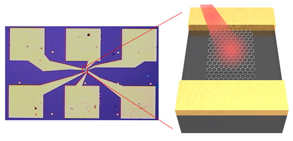
Photo credit: IBM Thomas J. Watson Research Center
I haven’t yet read the IBM submission, so my background understanding of this work is based on the Xia et al publication in Nature Nanotechnology and this useful Technology Review article. Here are some questions I’ll be pondering during the CLEO presentation:
First, in the Nature Nanotechnology paper, IBM reports that multiple graphene layers absorb light additively, with suspended bi- and tri-layer layer graphene absorbing 4.6% and 6.9% of incident light respectively . My question would be how far this can be stretched both theoretically and practically. Specifically, what are the outstanding manufacturing hurdles inhibiting the realisation of high absorption (>15%) structures?
Second, what is the wavelength range of the graphene photodetector and how does this change with bias conditions? Specifically, can it be modified to absorb down in the 650nm range to coincide with the transmission band of low-cost plastic optical fibers?
Third, how scalable is the epitaxial method developed by IBM to create the the graphene-on-SiC structures? When and under what conditions might wafer-scale deposition be possible?
Looking beyond CLEO, I believe IBM’s breakthrough has the potential to spawn a new industry based on epitaxial graphene and silicon photonics. Here are two off-the-cuff ideas for further investigation and innovation.
Epitaxial graphene on SiC
IBM’s photonics breakthrough is based on previous work from the same labs on the epitaxial formation of graphene layers on high-purity SiC wafers. I fully expect other researchers will strive to develop novel methods for enhancing the thickness and compositional uniformity of the graphene-on-SiC layers.
Graphene as LT-GaAs replacement for THz photomixers
IBM has already mentioned how its graphene photodiodes may be used in THz detectors. But could zero-bias graphene photodetectors also provide a low-cost alternative to LT-GaAs for use as THz photomixers? Preliminary measurements from IBM suggest the transit-time-limited bandwidth of a 200nm wide current generation region could be as high as 1.5 THz. It is not difficult to see how this could be packaged monolithically with a dual-wavelength laser to create an ultra-compact tunable THz source. Admittedly the THz power emitted by this device would be severely limited, but may prove adequate as a lab-on-chip spectrometer for biological, chemical and other analytical applications.
Overall I predict graphene will be a takeaway buzz word from CLEO 2010. I certainly look forward to learning more about this technology and its application to CMOS photonics.
Dr David Nugent is Founder and CEO of Elucidare Limited, a boutique technology development and investment advisory business.

Posted: 10 May 2010 by
David Nugent
| with 0 comments